The semiconductor industry is witnessing a paradigm shift as the back end of manufacturing becomes as technologically sophisticated as the front end. Among the most significant Semiconductor Back End Market Trends is the move from two-dimensional chip packaging processes to three-dimensional and 2.5D integration. This transition is driven by the slowing of Moore’s Law, which makes it increasingly difficult to shrink transistors further. Instead of scaling, the industry is stacking—placing multiple dies vertically or side-by-side in a single package. This trend is reshaping everything from equipment requirements to design methodologies and supply chain relationships.
Market Overview and Introduction
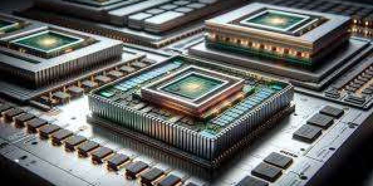
The most dominant of the current semiconductor back end market trends is the adoption of advanced chip packaging processes that enable heterogeneous integration. Traditional packaging simply protected a single die and connected it to a circuit board. Today’s advanced IC assembly techniques combine chiplets from different process nodes—logic, memory, analog, and RF—into a single system-in-package (SiP). These packages rely on wafer dicing and packaging methods that maintain extremely tight tolerances, as misalignment of just a few microns can ruin electrical connections. Semiconductor testing services have had to evolve to test these complex packages, which may have thousands of interconnects. Finally, backend semiconductor operations are being redesigned around cleanroom environments that rival front-end fabs, as contamination at the sub-micron level can kill a 3D package.
Key Growth Drivers
Several factors are accelerating packaging trends. First, the cost of advanced lithography (e.g., EUV) has become prohibitive for many applications, making chiplets and 3D stacking a more economical path to higher performance. Second, the need for high-bandwidth memory (HBM) in AI accelerators requires 2.5D integration with silicon interposers, a complex chip packaging process. Third, the demand for smaller form factors in mobile and wearable devices pushes IC assembly techniques to their limits. Fourth, the automotive industry’s need for high reliability drives adoption of fan-out wafer-level packaging (FOWLP), which eliminates the substrate and reduces failure points. Fifth, the rise of optical I/O for data centers requires hybrid bonding to achieve the necessary density.
Consumer Behavior and E-commerce Influence
Consumer behavior drives packaging trends through expectations of performance and portability. The desire for thinner laptops and phones with all-day battery life forces designers to use advanced chip packaging processes that minimize power consumption and height. E-commerce’s demand for faster cloud services has increased the market for AI accelerators, which rely on advanced IC assembly techniques. Consumers’ intolerance for device lag or crashes pushes manufacturers toward higher-performance packaging. Online reviews that compare device thickness and weight have made advanced packaging a competitive differentiator. Additionally, the trend toward foldable phones requires flexible chip packaging processes that can withstand repeated bending, a trend that is still emerging.
Regional Insights and Preferences
Semiconductor back end market trends vary by region. Taiwan leads in advanced packaging, with TSMC’s CoWoS (chip-on-wafer-on-substrate) and InFO (integrated fan-out) technologies setting industry standards. South Korea leads in HBM packaging for memory, with SK Hynix and Samsung driving 3D stacking of DRAM dies. China is aggressively developing domestic chip packaging processes to reduce reliance on foreign OSATs, with companies like JCET and Tongfu Microelectronics investing heavily. The United States is seeing a resurgence in packaging R&D, with Intel’s Foveros and EMIB technologies and government funding for the National Advanced Packaging Manufacturing Program (NAPMP). Europe is focused on automotive packaging, with Infineon and NXP leading in power module IC assembly techniques.
Technological Innovations and Emerging Trends
The most significant innovation in chip packaging processes is hybrid bonding, which eliminates solder bumps and creates direct copper-to-copper connections with pitch sizes below 10 microns. Another trend is the move from wafer-level to panel-level packaging (PLP), which uses larger rectangular substrates to reduce cost. In wafer dicing and packaging, stealth dicing and plasma dicing are replacing mechanical saws for thin, fragile wafers. Semiconductor testing services are adopting known-good-die (KGD) methodologies to ensure that chiplets are functional before assembly into expensive packages. IC assembly techniques for chiplet integration are being standardized by the Universal Chiplet Interconnect Express (UCIe) consortium, reducing fragmentation. Backend semiconductor operations are increasingly using inline metrology and inspection at every step, rather than only at the end.
Sustainability and Eco-friendly Practices
Sustainability is influencing packaging trends. Advanced chip packaging processes that enable higher integration reduce the number of separate chips and circuit boards, lowering overall material consumption. The move to fan-out packaging eliminates the organic substrate, which is difficult to recycle. Hybrid bonding uses less solder, reducing lead and tin consumption. In wafer dicing and packaging, laser-based methods produce less silicon dust and use fewer consumables than mechanical saws. Backend semiconductor operations are adopting solvent recovery systems for cleaning processes. Some OSATs are exploring biodegradable dicing tapes and recyclable shipping trays. Additionally, the energy efficiency gains from 3D integration (shorter interconnects mean lower power) contribute to sustainability.
Challenges, Competition, and Risks
Despite positive trends, challenges abound. Hybrid bonding equipment is extremely expensive, costing over $10 million per tool, limiting adoption to high-volume, high-margin products. The thermal management of 3D stacks is difficult, as heat-generating dies are stacked directly on top of each other. Competition among packaging approaches (fan-out, silicon interposer, embedded bridge) creates technology risk for OSATs that bet on the wrong method. The complexity of advanced IC assembly techniques has increased defect rates, reducing yield. Supply chain coordination is challenging when chiplets come from different fabs and must be assembled by a third-party OSAT. Additionally, the shortage of engineers skilled in both front-end and back-end processes is acute.
Future Outlook and Investment Opportunities
The future of semiconductor back end market trends points toward full 3D integration, with logic, memory, and sensor dies stacked vertically and connected by through-silicon vias (TSVs). Investment opportunities are strongest in hybrid bonding equipment and materials, as this is the fastest-growing segment of advanced chip packaging processes. Another area is design tools for 3D-IC, including thermal and mechanical simulation, as these are currently lacking. Startups developing new dielectrics and adhesives for chip-to-wafer bonding are attracting venture capital. Additionally, as panel-level packaging matures, equipment suppliers for large-substrate handling will benefit. The automotive sector’s need for high-reliability packaging will drive investment in advanced IC assembly techniques for power modules. Finally, the standardization of chiplets through UCIe will create opportunities for third-party chiplet suppliers, each requiring their own backend semiconductor operations.
Conclusion
In conclusion, the semiconductor back end market trends are unequivocally moving from 2D to 3D and from monolithic to heterogeneous integration. Chip packaging processes, IC assembly techniques, wafer dicing and packaging, semiconductor testing services, and backend semiconductor operations are all evolving to support this transition.
➤➤Explore Market Research Future- Related Ongoing Coverage In Semiconductor Industry: